
Stated simply, signal integrity (SI) analysis is the method of assuring that in a large digital system the pulsed digital signals generated by a source and propagated along an interconnect will reach the intended destination sufficiently distortion-free that it can be interpreted unambiguously by the receiving circuitry as either a “one” or a “zero” (e.g., as either a “high” or a “low” voltage). Also stated simply, power integrity (PI) analysis is the method of assuring that every circuit receives adequate power to operate as intended.
The SPPDG has been assembling large special purpose computer platforms since the early 1970s (see History). As early as 1973 we began to employ a digital logic family in our digital system designs referred to as Emitter Coupled Logic (ECL) 10K, that could support up to 40 MHz system clock rates, and with rising and falling edges on the digital waveforms of 2 nanoseconds (nsec). Early laboratory tests demonstrated that two problems had to be overcome: care needed to be taken in the interconnects between chips to assure that the conformation of the pulsed waveforms would not be so degraded that the destination chip’s circuitry could not decide whether the signal was a “zero” or a “one”. The same laboratory tests demonstrated that the so-called “return-path currents” in the power and ground planes of the circuit board could be significantly degraded if the inductances in the power and ground plane paths were too high. Accordingly, we developed specific set of implementation rules that governed how the circuit boards themselves should be designed, and how the wiring interconnects between chips were to be constructed.
Early power integrity design rules for ECL 10K chips: We worked with Augat, Inc. to design and have them fabricate for us so-called “wire-wrap boards” with multiple buried power and ground plane layers, and with the maximum amount of metallization on each power or ground plane layer (the wire-wrap pins penetrated the metallization with only a small pullback of the metal from each pin, rather than removing an entire row of metallization around a set of pins). We installed decoupling capacitors between the supply voltage planes and the ground planes at the location of each and every integrated circuit.
Early signal integrity design rules for ECL 10K chips: We controlled the height of the interconnect wires above the metallization planes to maintain, as best possible, a constant interconnect impedance of roughly 75 ohms, i.e., a controlled impedance interconnect structure. We “terminated” every interconnect in the characteristic impedance of the interconnect (roughly 75 ohms) to prevent voltage reflection waves from degrading the signal waveforms. For the fastest and most sensitive signals (e.g., clock signals), we employed either differential twisted pair signaling, or in some cases small-diameter 75 ohm coaxial cables. All signal interconnects between circuit boards in an electronics drawer, and all signal interconnects between drawers in a cabinet, or between cabinets, were transmitted as differential twisted pairs or on paired coaxial cables, thereby to eliminate slight differences in the ground and power plane voltages between the boards, drawers, or cabinets.
Conversion to ECL 100K chips: In the late 1970s we transitioned from ECL 10K to the much faster family, ECL 100K, which could sustain system clock rates in the 1 GHz range, with signal rising and falling edges of 0.7 nsec. These faster clock rates and shorter signal risetimes increased the design challenges of our digital systems that employed the ECL 100K family. The earlier design rules described above were made more stringent; for example, a much higher percentage of point-to-point interconnects on a wire-wrap board were converted to differential twisted pairs; and for the fastest systems, we bore the added cost of design and fabrication of multilayer printed circuit boards to replace the wire-wrap structures, with buried signal interconnect layers sandwiched between power and ground distribution planes. This conversion better controlled the interconnect impedances and decreased instantaneous voltage fluctuations on the power and ground plane layers. We paid much more attention to the dielectric materials employed in the decoupling capacitors located at each chip (described above), since we learned that some dielectrics exhibited degraded capacitance functionality at higher clock rates than other materials. We developed improved termination resistor packs with lower internal inductances. Finally, we converted our chip packaging from dual inline packages to leadless chip carriers, thereby to reduce the series inductances in the packages themselves (see the companion descriptions in the History section of this web site). These design approaches were thus fairly mature by the early 1980s, when we converted many of our designs from the various families of ECL to gallium arsenide (GaAs) integrated circuits, which could support system clock rates in the 2-3 GHz range.
Creation of a SI/PI Design Team: During the 1970s and 1980s most of our high speed design rules, as described in the prior paragraphs, were developed from laboratory measurements and ad hoc decisions based on experience, and where possible on crude models fed into early versions of the SPICE simulation tool. However, by 1990 it became clear that these ad hoc design rule approaches would no longer suffice as system clock rates continue to increase and signal risetimes continued to decrease. Thus we created, within the SPPDG, a specialized team of SI/PI engineers to develop tools and design rules in a more rigorous fashion, based upon detailed software simulations of the structures to be developed, at the chip level, the chip carrier level, at the circuit board level, and even at the drawer and cabinet levels. The following sections describe the present status and capabilities of SI/PI analysis capabilities within the SPPDG at the present.
Applications such as numerical processing, database queries and graphical visualization often require the highest computing capability available. Due to progressing technology limitations, computer architects have relied more heavily on using multiple processors, both within single computer chips and across multiple chips, in order to advance computational capabilities. Multiple processors, along with multiple computer memory systems must be designed to inter-communicate at very high digital data rates; otherwise the overall computational speed of a computer system is diminished.
In the early 1990’s, the SI focus was mainly on parallel busses. For example, we would analyze the I/O paths from a 1 Gigasample per second (Gs/s) 8-bit analog to digital (A/D) computer driving an 8:128 demultiplexer, slowing down the 1 GHz 8 bit bus to a 128 bit bus switching at 62 MHz; the latter data rate was then slow enough to interface with field programmable logic chips. SI challenges for wide parallel buses include: a) constricted design so that all signals within each bus are synchronous (i.e., they require nearly the same electrical delay to communicate with a synchronous chip); b) determination of adequate physical separations between neighboring signals to minimize coupled noise (crosstalk); c) selecting proper termination techniques so that signals are not reflected, thereby degrading part of the incident signal; and d) provision of any guidance needed to ensure that multiple signals do not switch in-phase, thereby causing timing push-out (the “simultaneous switching noise (SSN)” problem).
Around the Year 2000, serializer/deserializer (SerDes) circuit technologies emerged to enable high bandwidth connections between the various printed circuit boards within a cabinet and between nearby cabinets. These original SerDes links typically operated at roughly 1 Gigabit per second (Gb/s). The SerDes link serializes a wide parallel bus into a much higher data rate serial link to realize an order of magnitude increase in I/O bandwidth per signal connection.
The SerDes data rates and number of SerDes links per chip have increased substantially since the Year 2000. For example, in 2015, high performance processing chips run at data rates as high as 32 Gb/s with as many as 48 SerDes links per chip, so that greater than 1 Terabit aggregate performance can be obtained from a single computer chip.
The SI challenges with dense, high data rate designs are significant. The copper signal paths and surrounding insulating media have significant loss for 32 Gb/s signals. A 1-volt transmitted signal is typically degraded to around a 0.050-volt signal at the receiver due to metal and insulation losses. Materials must be selected and rules provided to keep material losses low and signal paths adequately short so that signal degradation does not exceed the signal recovery capabilities at the receiver. The entire signal path must be simulated to optimize metal size and cross-sectional shapes for acceptable signal transmission. Failure to do so causes portions of the signals to reflect to and fro along the signal path (like echoes) to distort the intended signal.
Both SerDes link simulation and measurement utilize “eye diagrams” as a means to determine link quality. In an eye diagram hundreds or more digital signal periods (of receiver voltage versus time) are superimposed upon one another to create a pattern such as that shown below (Fig.1). The center opening size in the eye diagram provides a measure of expected error rates for the SerDes link. In this case the SPPDG investigated “active repeaters” to capture a severely degraded signal and boost the signal back to the 1-volt level, and then retransmit it to the final destination. Therefore the use of a repeater effectively doubled the distance between source and destination chips, which can offer performance advantages in some architectures. This repeater was targeted to run at 20 Gb/s in the Year 2010 time-frame.
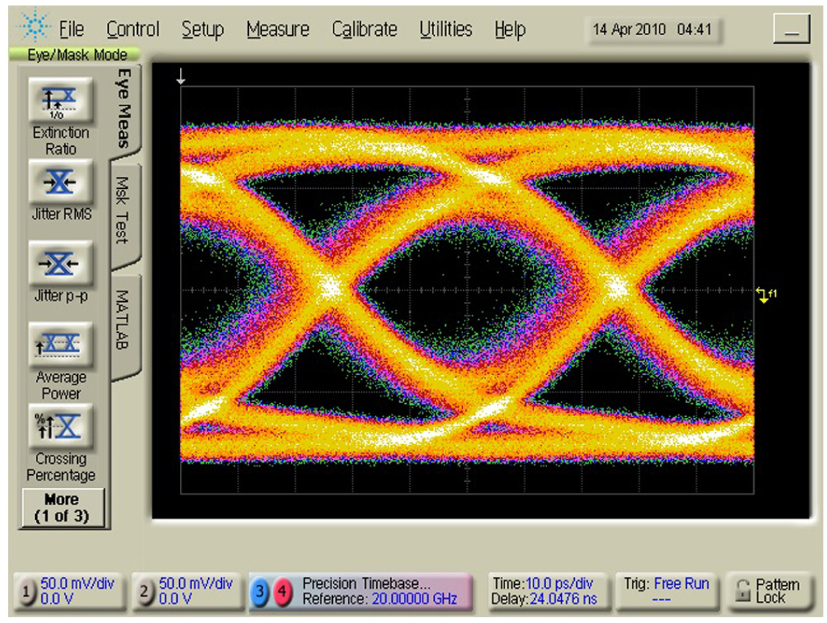
Fig.1 20 Gb/s eye diagram of output from Mayo designed repeater/buffer chip.
SerDes technology has not replaced parallel bus intercommunication. In fact, parallel bus clock rates in the Year 2015 are approaching 3 GHz. Chip designers have implemented clever techniques to delay or speed up and align signals within the same bus to keep them synchronous. However, at the higher bus speeds, crosstalk and other design considerations become increasingly important.
An industry trend has been the inclusion of multiple chips on the same package, similar to the “multi-chip” module technologies from the late 1980’s. These technologies require very high aggregate bandwidths between chips on the same package, without the power, latency, and complexity of a SerDes link. The SPPDG investigated a “crosstalk cancellation” approach that allows signals to be placed in close proximity to one another yet offer low bit-error-rates despite the high levels of crosstalk associated with tightly coupled signal paths. Eye diagrams are shown below (Fig.2) for worst and best case switching patterns for a 12-wire interconnect (with, presented as a reference, a 6-wire example, using conventional spacing for low crosstalk in the same board area as that used for 12-wire case), using a standard termination approach versus a crosstalk cancellation approach.
Fig.2 Crosstalk cancellation eye diagram results for 6- and 12-wire bundle configurations operating at 16 Gb/s.
At various speed/distance cross-overs, electrical signaling becomes too difficult due to the loss of copper signal paths. Since the late 1990’s the SPPDG has modeled, tested, and demonstrated various optical communication technologies. As data rates continue to increase, optical communication will be required to replace progressively shorter electrical paths. However, SI analysis will be essential for designing these electrical/optical interfaces.
Moore’s Law drives contemporary system designs to ever-increasing levels of integration using smaller and smaller semiconductor devices operating at lower and lower voltages. Exponential growth in the number of these devices results in integrated circuits which can vary their dissipation by tens to hundreds of watts in an interval as brief as a few nanoseconds. This variation in power causes a corresponding variation in the current from the power source and leads to instantaneous variation in the supply voltage, which can disrupt the delicate timing of digital circuits and cause malfunction or failure of entire systems. Power Integrity is the task of preventing such malfunctions by meticulous analysis and design of the power delivery network to ensure that all supply voltages are maintained within acceptable limits.
Since load currents change much faster (~1000x) than voltage regulators can respond, it is necessary to provide supplemental charge-storage in close proximity to the sensitive circuits. These charge-storage capacitors supply the instantaneous current required to maintain the local voltage while the regulator reacts. Selection of these capacitors is governed by the voltage-variation limits of the circuits being served, along with specific characteristics of the components and the conductors which connect them to the load, using a design technique commonly called the Frequency Domain Target Impedance Method. As shown below (Fig.3), specific capacitors are added to the network to ensure that the effective impedance of the network is below a maximum “target” impedance, which in turn constrains the maximum voltage variation that the network can induce when load currents change.
Fig.3 Power plane decoupling using frequency domain target impedance method (FDTIM).
In addition to constraining supply-voltage variations, power integrity analysis seeks to avoid the creation of thermal “hot spots” that can arise as a result of Joule heating of conductors when tens or hundreds of Amperes are distributed among system components. The figure below (Fi.4 illustrates the estimated still-air temperature-rise on a printed circuit board when the 195 Amp ASIC-supply current flows through a constriction. Local heating such as this could lead to failure of the insulating layers in the board and catastrophic destruction of the system.
Fig.4 A map of current density in printed circuit board conductors for an application-specific integrated circuit (ASIC) drawing 195 amperes, showing estimated temperature elevations at various locations on the printed circuit board.
Moreover, high currents can produce significant voltage gradients between integrated circuits and across individual circuits themselves. These voltage gradients further reduce the allowable voltage variations and compound the design of the capacitor network, which in turn increases the physical size of the circuit board and increases system cost. The image below (Fig.5) depicts a 4.7 mV gradient across the ASIC, which wastes nearly ten percent of the total voltage margin for this design.
Fig.5 Expanded view of a section of the previous diagram, but here showing voltage gradients across the ASIC and in the region on the circuit board in close proximity to the ASIC.
SI/PI challenges have become much more intense in the last few years as transistor dimensions shrink and on-chip transistor counts increase. Given that the newest chips are fabricated with sub-22 nm transistors, and a conversion to vertical rather than planar devices has taken place. We are now working with single chips dissipating more than 400 W, at very low supply voltages. Concomitantly, in-package and on-board power dissipations are increasing dramatically, in turn creating difficulties in maintaining low-noise power rails, especially when confronted with rapid current transients caused by the high-power chips. This evolution is driving us to develop new SI/PI analysis tools (e.g., #346 in the Publications section of this web site), including a new time-domain-based deep-analysis approach for selecting and siting decoupling capacitors on a high-power circuit board (to be published in 2021). It is of historical interest that SI/PI analysis, introduced to the electronic systems community three decades ago, continues to increase in importance to the present.
Information updated Friday, October 16, 2020
Any use of this site constitutes your agreement to the Terms and Conditions and Privacy Policy linked below.
"Mayo," "Mayo Clinic," "MayoClinic.org," "Mayo Clinic Healthy Living," and the triple-shield Mayo Clinic logo are trademarks of Mayo Foundation for Medical Education and Research.