
The Special Purpose Processor Development Group was founded at the Mayo Clinic in 1971. Throughout the 1940's, 1950's and 1960's, the Mayo Clinic had conducted research on a variety of diagnostic techniques for diseases of the heart and lungs using continuous motion "biplane" X-ray video imagery, followed by analog electronic processing (and later, computer processing) of these image streams to diagnose cardiopulmonary diseases. In the late 1960's and early 1970's, this work led to the development of a conceptually advanced, experimental X-ray computed tomography (CT) imaging machine, the Dynamic Spatial Reconstructor (DSR). Of current interest is the fact that the DSR was so far ahead of its time that only in the past 5-7 years have helical-scanning X-ray CT machines such as the Siemens SOMATOM and GE LightSpeed offerings begun to approach the four-dimensional spatial and temporal resolution of the original DSR.
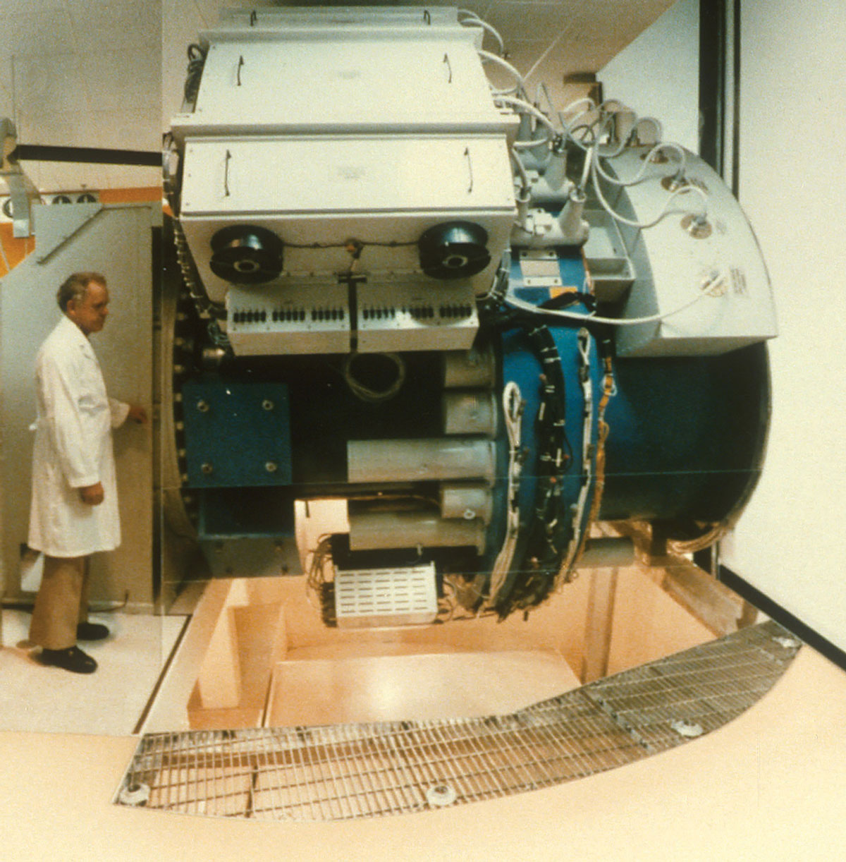
The final version of the DSR was installed in the Medical Sciences Building on the Mayo Clinic Rochester campus in 1978. This machine produced raw image data at 200 million 8-bit picture elements (pixels) per second. The raw data then required a large amount of computer processing (approximately 1000-10,000 arithmetic operations to convert a "raw" data pixel into a final X-ray CT image pixel), (e.g., ten seconds of collected data required many months of processing on mainframe computers to achieve the three dimensional X-ray tomographic imagery which the research group was trying to achieve). Dr. Barry Gilbert (former Director of the SPPDG) began work in 1971 on the designs for special purpose parallel-architecture computers (which presently would be referred to as “High Speed Computers, or “HPCs”) which would be able to process data collected by the DSR in only 20-40 times longer than the data collection period itself (e.g., ten seconds of raw data processed within 200-400 seconds, rather than many months on the conventional computers of the day). Such high computational throughput rates would require 80-100 billion arithmetic operations/sec, five orders of magnitude beyond the then state of the computer art.
With the need to solve the DSR computational problem as the initial emphasis, Dr. Gilbert assembled a design team with the expertise to develop this technology, with funding from the National Institutes of Health (NIH). In addition to a concentration on improved X-ray CT algorithms and parallel processing computer architectures to execute these algorithms, Dr. Gilbert's research group relied upon and worked to develop further the fastest digital integrated circuit (IC) technologies as a potential partial solution to these high throughput problems, an emphasis which has continued unabated for the past 45 years.
The first project undertaken by the new computer research group, in 1972, was the development of a star-architecture digital network computer, the High Speed Interface, which was capable of interconnecting up to eight different mainframe and special purpose processors.
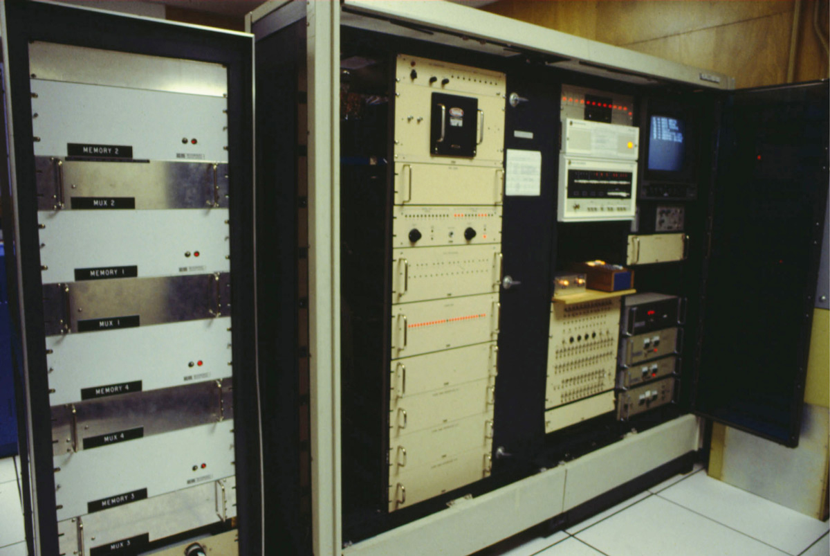
The "data path" to each of the eight computers on this synchronous star network, driven by a 40 MHz four-phase distributed clocking system, could transfer up to 40 million 16-bit words per second (80 megabytes/sec) in each direction (i.e., full duplex transmission) from one or two data sources on the network, to one to (up to) eight destinations, under program control. For purposes of comparison, in 1972 the early microprocessors of that time were operating at 100-200 KHz clock rates, and only the Cray 1 supercomputer was planned to operate at system clock rates and data transfer rates equivalent to those of Mayo's High Speed Interface network processor. The "hub" of this star network processor contained four fully programmable stages of pipeline processing (shift matrix, lookup table, binary format converter, and arithmetic logic unit--or "ALU") which, for 8-bit or 16-bit data words, were capable of achieving a combined processing rate of 160 million 16-bit fixed-point arithmetic operations per second. The entire system was controlled on a clock cycle by clock cycle basis by a loadable 7 nsec wide-word microprogram control store, the first such implementation ever reported.
The star processor, which filled three specially fabricated electronic relay racks, was assembled from more than 3000 ECL 10K (emitter coupled logic) and ECL 100K integrated circuits mounted on thirty circuit boards. A description of this star network processor appeared in IEEE Transactions on Computers, November 1976 (#18 and #19 in the Publications list). Several smaller processors were also developed, comprised solely of the faster ECL 100K parts, which operated at clock rates in the 200-250 MHz clock rate range. Although these prototype processors addressed a portion of the processing problems created by the experimental tomography units being developed at Mayo, it soon became clear that additional processing speed would be required if such advanced computed tomography units were to become practical and cost effective.
Laboratory testing at Mayo eventually revealed that the limitation in the performance of the ECL 100K chips was the packages into which they were typically installed by the chip manufacturer. To address the problem of the IC packaging limiting the performance of the ICs themselves, during 1976-1978 Mayo performed evaluation studies on many different commercially available IC packages. The resistance, inductance and capacitance measurements conducted at Mayo revealed that the leads of the dual-inline packages (DIPS) (and, to a somewhat lesser degree of the flat package, FPs) exhibited very high values of inductive and capacitive parasitics. Since the primary concerns of the packaging industry at that time were purely in regard to the mechanical aspects of the packages, with virtually no attention given to the electrical issues (with the possible exception of DC lead resistance), many of the packages simply could not perform well at higher frequencies.
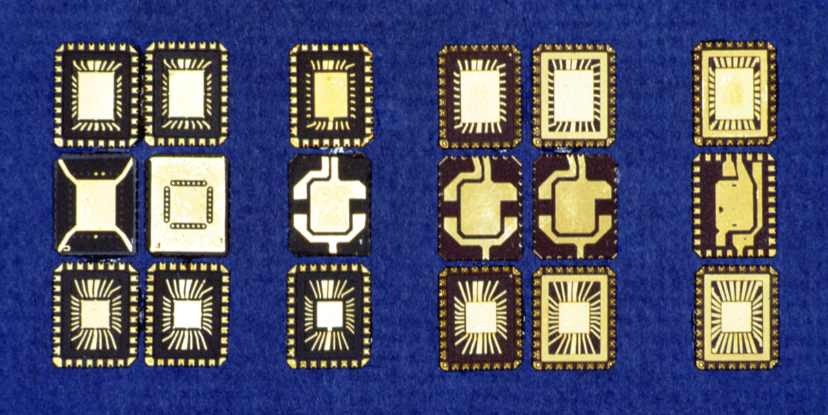
To address the high frequency AC packaging issues, in 1979 the Mayo group began the design of a family of custom leadless chip carriers, with serious attention given to their high frequency behavior. This family of chip carriers was designed to be used with both ECL 100K logic and memory components, thus requiring two different die (die refers to an unpackaged IC) cavity configurations, yet with a common input/output (I/O) pin footprint. This approach to the design of the packages in the family assured that a single package footprint could be used on the system boards to accommodate both package types.
Early gallium arsenide (GaAs) components designed by Mayo were targeted for this package as well. Many different versions of the package, comprising an entire family, were designed and fabricated, utilizing multiple vendors. The evolution of this package design was based almost totally on measurement results from each previous version thereof, because of, at that time, a near total lack of suitable electromagnetic computer aided design (CAD) simulation tools. Over a four year period (1979-1983), the original package evolved from a minimized parasitics version to a controlled impedance version with power/ground plane construction, in-cavity and back surface power supply decoupling, and signal termination. The final complete family contained nearly thirty slightly different versions of a common chip carrier footprint, each version emphasizing a different set of strengths and limitations.
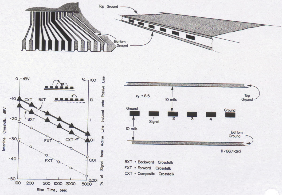
Coordinated with the 28 I/O chip carrier design was the development of high frequency prototyping printed circuit boards (PCBs) for developing high performance systems. The early versions of these printed circuit boards contained a power and ground plane sandwich construction, varying from three to twelve power/ground layers, but no buried signal layers. All signal connections were made with twisted pair wirewrap wire, which provided a moderately controlled 75 ohm impedance transmission line environment for each signal net.
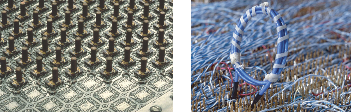
In conjunction with the prototype boards, custom terminator resistor networks were developed and capacitors were characterized to determine which materials and case styles performed the best over a broad frequency range. The combination of the chip carriers, specially designed circuit boards, and specialty components resulted in wire wrapped ECL circuits that operated as high as 570 MHz clock rates and direct, point to point, wired GaAs circuits which performed at over 1 gigahertz (GHz) clock rates.
The completion of the 28 I/O package family was followed in the early 1980's by SPPDG's development, for chips with higher pad counts, of four different types of 88 I/O packages (cofired alumina, cofired beryllia, single layer and metalization [SLAM] alumina, and thin film metalization on alumina), followed in the mid 1980's by a thin film 216 I/O package with 192 integral termination resistors. The ten year effort to create single chip packages for high performance integrated circuits eventually was terminated after the development of a 240 I/O elastomer mounted package of dimensions .750 inches square. Each of these packages had a companion prototyping board, with prototype components that operated in the 500 MHz to 1 GHz range.
During the development of the single-chip packages described above, it became clear that irrespective of the quality of the design of any given single-chip package, the package imposed significant electrical performance constraints on the chips because of residual parasitic inductance and capacitance, and on the circuit boards and the resulting signal processor systems because of the large amount of real estate consumed by the packages (package areas were 15-60 times the areas of the chips themselves). The solution to these electrical and mechanical problems was the complete elimination of the IC package, and a conversion to multichip packaging approaches such as hybrids and multichip modules (MCMs), which may be thought of as microminiature circuit boards, on which bare integrated circuits are installed and connected to extremely narrow traces on the surface of and buried within the MCM.
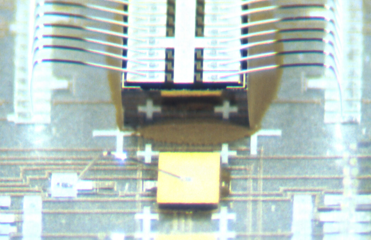
In 1987 the SPPDG began investigating several potentially viable MCM technologies for use in the packaging of multiple bare chips (die) on the same microminiature circuit board (i.e., MCM) substrate. Based on past experiences with cofired ceramic single chip packages, as well as with many advanced printed circuit board technologies (similar to what is now referred to as MCM-Laminate [MCM-L]), it appeared that the MCM-Deposited (MCM-D) technology offered the most promising option for high clock rate signal processor systems. A two-step process was undertaken to evaluate the new MCM technologies. First, MCMs with passive interconnect line structures were designed and fabricated. These first experimental MCMs became known as passive test coupons, with each serving as the characterization vehicle for one of the MCM technologies. The second step was the design of active circuit demonstration modules using high performance GaAs chips. The very first MCM designed at Mayo was a combined passive/active vehicle; it was fabricated in 1988.
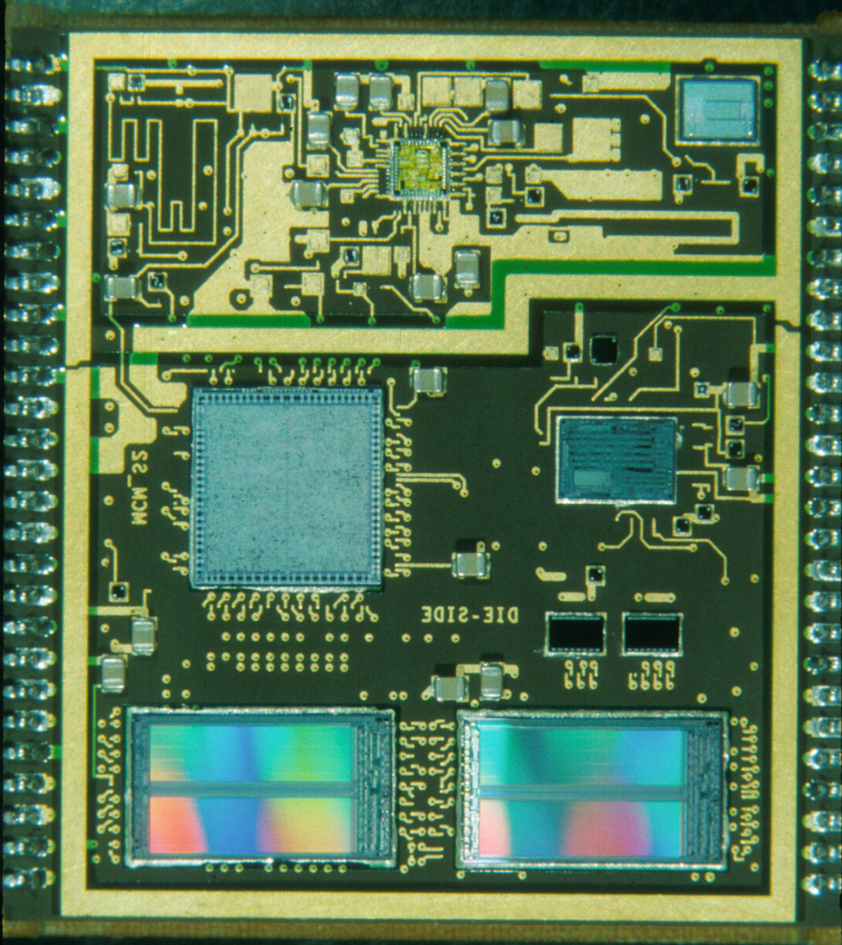
The SPPDG evaluated more than a score of different MCM technologies throughout the 1990's, and developed significant expertise in design, assembly, and testing of modules and systems based on this packaging concept. In addition to the digital signal processing applications for which the initial MCM studies were performed, many analog and mixed signal modules were design and tested, exploiting the inherent advantages of MCM packaging. The miniaturized global positioning system (GPS) receiver pictured here, for example, actually had slightly better performance than the traditional circuit board implementation of the same circuits.
In the early 1980's a new technology for ICs began to emerge, which appeared to be capable of even higher speed operation than the silicon ECL families. This technology was gallium arsenide (GaAs). The Defense Advanced Research Projects Agency (DARPA) was interested in exploiting this new GaAs technology for use in high speed signal processing applications, which had many of the same requirements as the Mayo DSR application. DARPA began funding Mayo SPPDG in 1980 to press the state of the art of the GaAs technology by developing computer aided design (CAD) tools that could be used to design GaAs ICs; the Mayo group also designed a set of GaAs proof-of-concept test chips as well.
Throughout the 1980's four GaAs "pilot lines" were created to improve the GaAs chip fabrication technology; Mayo provided design support to all of these fabrication facilities. The transistors developed for this first generation of GaAs integrated circuits were so-called metal-semiconductor field effect transistors (MESFETs).
The first few test circuits contained simple arithmetic functions, such as multipliers and adders, as well as representative portions of high speed signal processor architectures (e.g., ALUs). The number of gates that could be successfully implemented on a GaAs MESFET circuit, and hence the limit of these test circuits, was on the order of a few thousand (between 1000 and 6000). By the late 1980's, GaAs MESFET chip technology had matured sufficiently that custom circuits operating in the 1-2 GHz range could be acquired from several commercial suppliers.
From the mid 1980's to the mid 1990's the integrated circuits industry developed GaAs integrated circuits exploiting so-called heterojunction bipolar transistors (HBTs), which had higher fT and fMAX values (65-75 GHz) than GaAs FETs, but required more power per logic function. Working in collaboration with Rockwell and other fabricators, the Mayo team designed a number of GaAs HBT chips which operated at up to 12 GHz clock rates, although the gate counts available on these GaAs HBT integrated circuits was in the range of 1000.
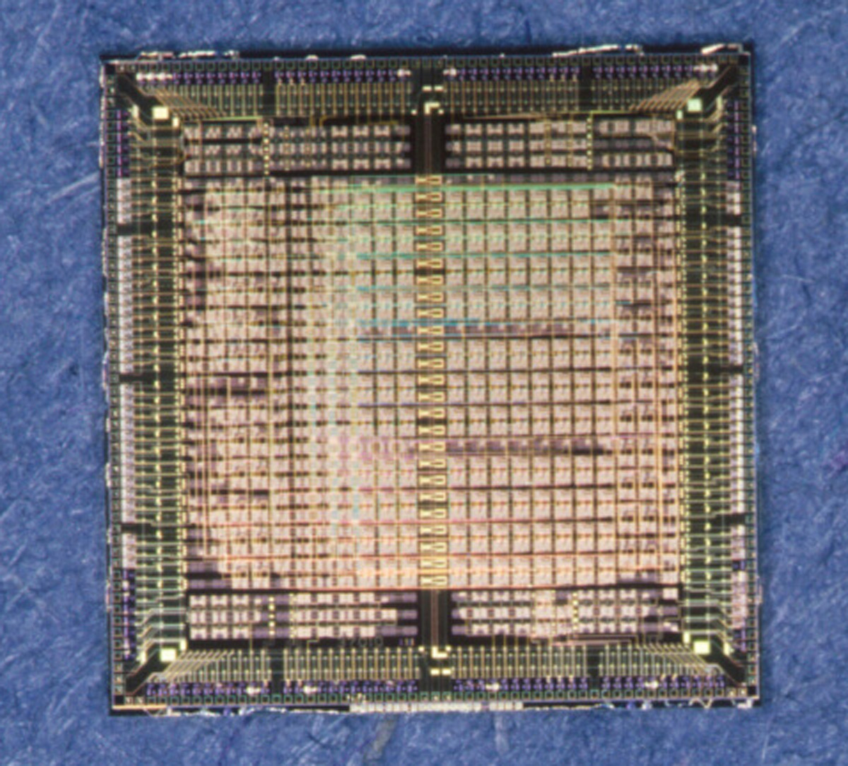
Since the early 1980's, the SPPDG has designed more than 400 integrated circuits in more than a dozen of different technologies, including conventional "bulk" silicon (Si), silicon on insulator (SOI), silicon germanium (SiGe) BiCMOS, gallium arsenide (GaAs), indium phosphide (InP), antimonide-based compound semiconductor ("ABCS"), and wide-bandgap gallium nitride (GaN) devices. The circuits have ranged in complexity from single device characterization structures to multi-million transistor signal processors. Applications of these circuits have included technology evaluation, signal and data processing, computation and communications.
Electronic computer aided design (ECAD) tools have played a crucial role in electronics development since the 1970's. Early circuit simulation programs such as SPICE helped design engineers analyze and optimize their proposed circuit designs to reduce prototyping effort and improve system performance. Since that time, assortments of CAD tools have evolved into complete integrated design frameworks for integrated circuits and printed wiring boards (PWBs). Many of these systems are very sophisticated, and serve the design needs for a wide variety of engineering disciplines.
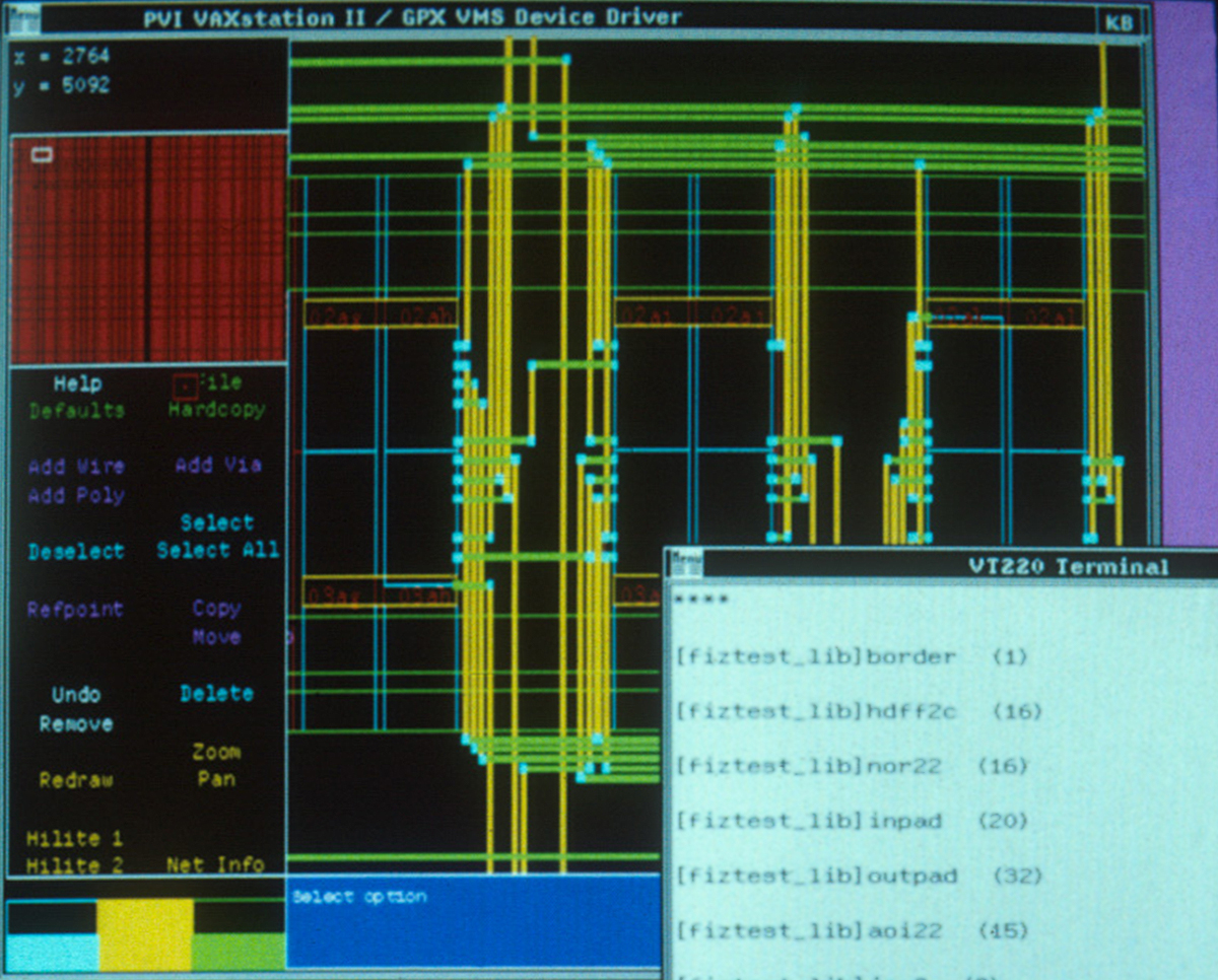
The SPPDG found itself in need of specialized ECAD tools to assist in the design and simulation of high performance non-silicon digital integrated circuits, and systems constructed with these specialized chips, in the early 1980's. There were few ECAD tools and NO design frameworks at that time, so it was necessary to develop the appropriate tools and supporting framework to assist in the design and implementation of high clock rate digital signal processors. The Mayo-developed tools became an integrated system called MagiCAD.
The SPPDG used MagiCAD almost exclusively for semicustom GaAs IC design from the mid-1980's until 1998. By that time, simply maintaining the complex infrastructure of an ECAD system became a significant effort. Meanwhile most of the major commercial ECAD vendors had improved their tool suites significantly, adding flexibility and support for "deep sub-micron" features which were similar to the design issues in high speed GaAs IC design. Today Mayo SPPDG has many different commercial ECAD tools for semicustom IC, PWB, and MCM design available in-house, although several tools and scripts developed in-house are still relied on.
One important component of high clock rate system design is attention to the details of the electronic packaging into which the high performance integrated circuits are installed.
By the mid-1970's it was clear to the Mayo group that inductive and capacitive parasitics in the single chip packages employed for silicon ECL components, as well as the interconnect between these high performance chips, significantly reduced the performance of an overall system. This realization led to a series of IC package and prototype designs with the primary goal of fully exploiting the capabilities of the ECL chips. Early package prototyping required fabrication and testing of chip carriers to determine if the packages met the system design goals.
The Mayo SPPDG began developing electromagnetic simulation tools in 1980 to create a capability to predict the parasitic capacitances and inductances in both the chip carriers and the intervening interconnect. By 1985 the development of Multilayer Multiconductor Transmission Line (MMTL) Analysis tools created the capability of predicting, with a high degree of accuracy, the performance capabilities of inter-chip interconnect. Several versions of MMTL were created for lossy and loss-free transmission line analysis. Single chip package prototyping was then conducted in simulation, and it was possible to create new chip carrier designs using these tools. The tools themselves were made available to the entire community through postings in open-source repositories.
The SPPDG has continued to develop and deploy a number of ECAD application programs and integration scripts to enhance the performance of the various commercial design systems in use today. These tools range in complexity from simple scripts (e.g., generate piecewise linear HSPICE models for pseudo-random bitstreams) to complete engineering tools based on new techniques and algorithms (e.g., new measurement de-embedding analysis tools, and new tools for signal integrity and power integrity analyses). Once new algorithms and techniques are implemented, they are generally listed in the Publications section of this web site.
The current research mission of the SPPDG continues essentially unchanged from the early 1970's, though the technology has evolved considerably at all levels. As early as 1974, the group worked on and has been concerned with the design of advanced-technology, very high clock rate digital integrated circuits and high center-frequency analog and mixed-signal integrated circuits; the development of ECAD and electromagnetic simulation tools for very high clock rate digital signal processors; the electronic packaging, assembly and test of high performance integrated circuits, computer and chip-level architectures; the demonstration of novel prototype digital, analog, and mixed-signal special-purpose processors; and the investigation of any other fields or technologies which can contribute to the development of processors with very high processing bandwidth or computational throughput.
The SPPDG moved from the downtown Mayo campus to a new off-campus Mayo-owned facility in 2001. SPPDG’s space contains multiple clean rooms and other physical resources to support advanced electronics research. The facility has evolved into a world-class electronics research laboratory, with design, assembly and test capabilities in many advanced technology areas.
Any use of this site constitutes your agreement to the Terms and Conditions and Privacy Policy linked below.
"Mayo," "Mayo Clinic," "MayoClinic.org," "Mayo Clinic Healthy Living," and the triple-shield Mayo Clinic logo are trademarks of Mayo Foundation for Medical Education and Research.