SPPDG has a suite of assembly tools for the purpose of creating proofs-of-concept, fabricating test vehicles to support design, modeling, and simulation efforts, and building prototypes for field trials. Assembly capabilities include packaging integrated circuits (first level packaging), assembling printed circuit boards (2nd level packaging), and building sub systems (3rd level packaging).
In addition to assembly, SPPDG has capabilities to rework packages and to perform failure and constructional analysis. Processes have been developed to remove and replace components and solder attached packages from PCBs.
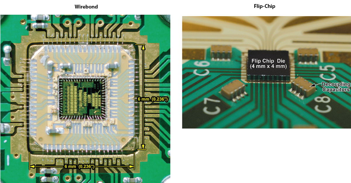
The assembly laboratory provides high-end first level packaging capability for prototyping new chip designs. Integrated circuits (IC) can be attached face up and wirebonded or face down and flip-chip attached to a single or multi-chip package. Wire bonding is performed on a gold ball bonder, with the capability of attaching down to a 0.7 mil bond on minimum pad dimension of 2.5 mils on a side. Flip-chip attach can be done with solder, conductive adhesive, or gold stud bump (thermocompression and thermosonic bonding).
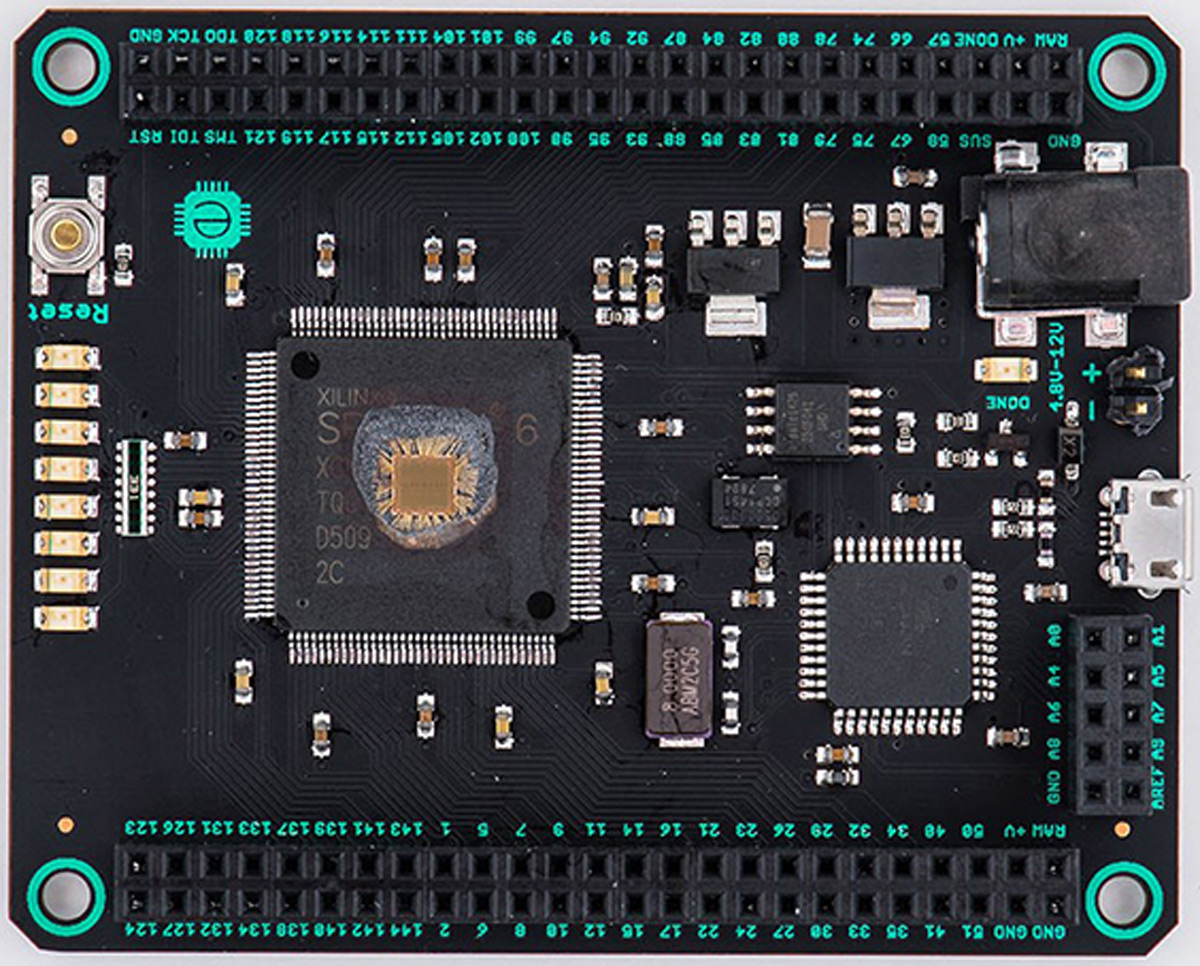
IC Bonding Examples
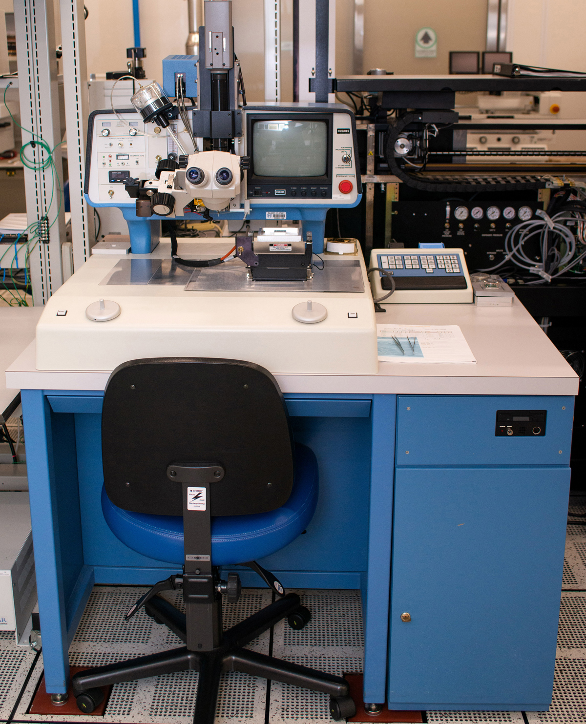
Palomar 2460-V Ball Bonder
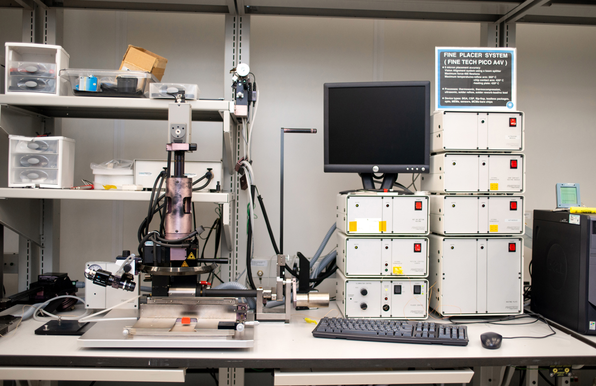
Finetech Pico Flip-Chip Bonder
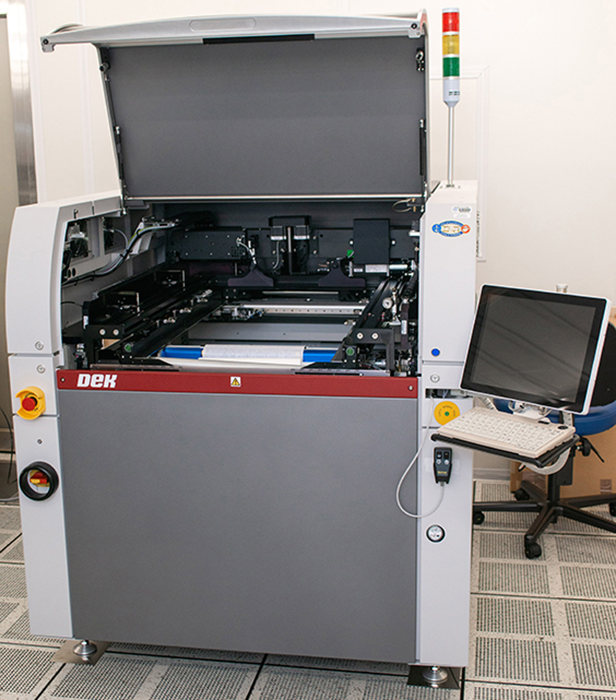
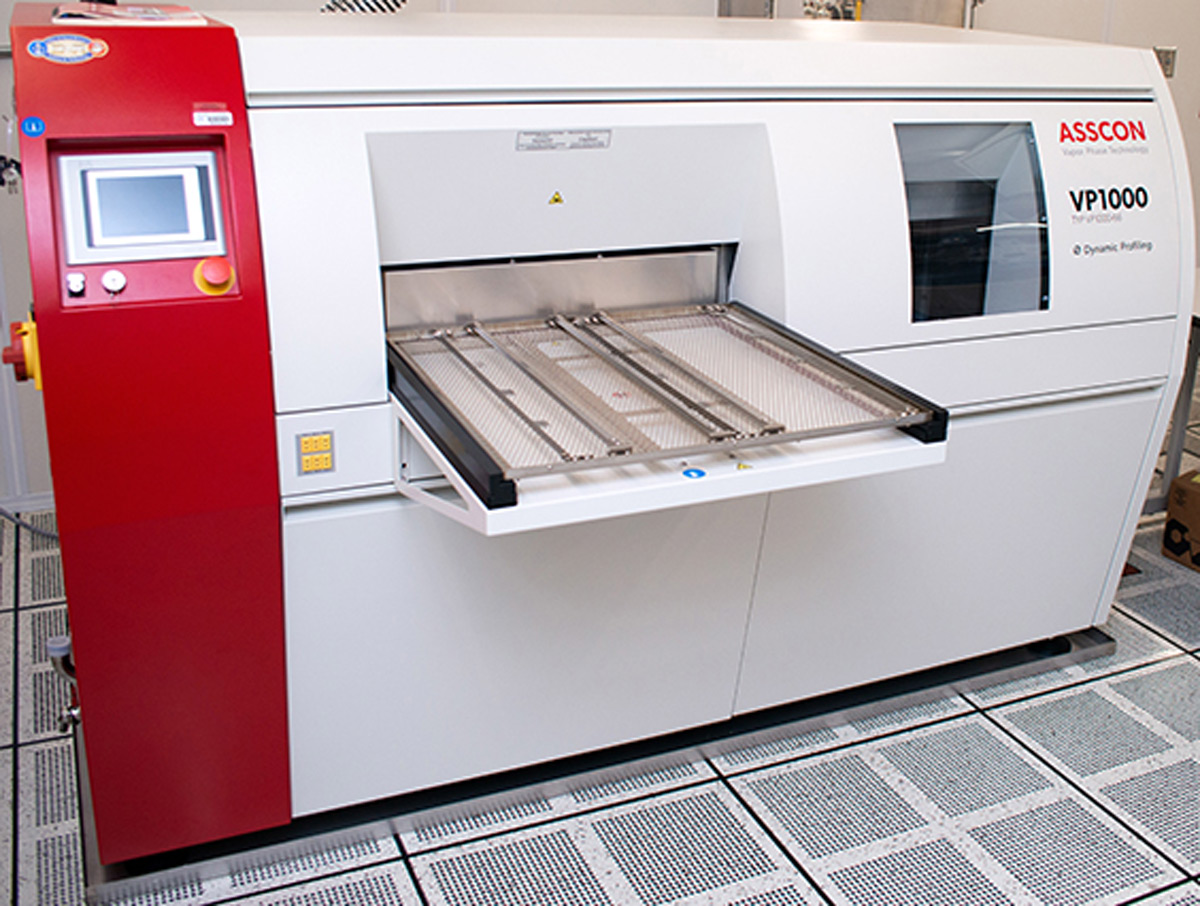
The SPPDG assembly lab is equipped to assemble a range of surface mount (SMT) and pin-in-hole components including packaged and bare die ICs and discrete components,connectors. Assembly can be done with leaded and lead-free solders as well as epoxies. Solders can be screen printed or dispensed manually and then reflowed either in a vapor phase reflow system or in the case of low temperature solders, in a 4-zone convection oven. Our SMT equipment can handle board sizes of up to 10” (w) x 7” (l) x 0.100” (t). We have the capability to perform 2-sided board assembly of up to 480 components with a minimum component size of 0201.
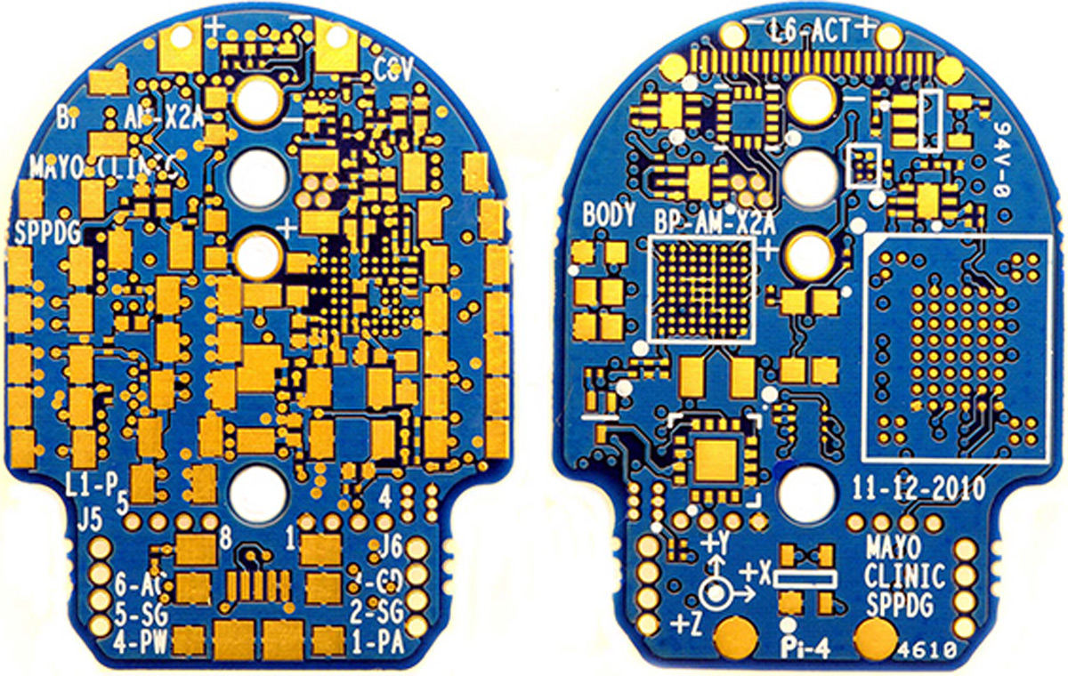
Fully Assembled PCB Example
Screen Printer
Vapor Phase Reflow
Westbond Pick & Place
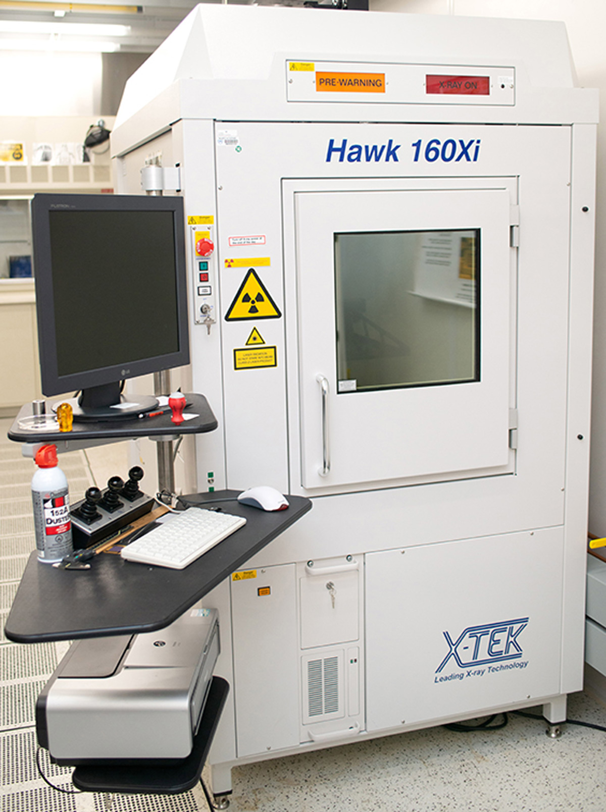
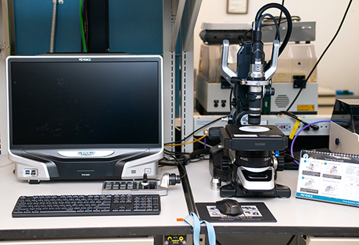
The SPPDG assembly lab is equipped to inspect and measure parts through the assembly process. In addition, the lab has the capability to analyze packaged parts, looking at inner layer construction as well as defects. Inspection of flip-chip and BGA parts is performed on an X-Tek Hawk X-ray inspection system. In addition to optical microscopes with precision 3D stages for taking measurements, the lab is equipped with a Keyence VHX-6000 3D microscope.
X-Tek Hawk X-Ray Inspection System
Keyence 3D Microscope
Delidded Package
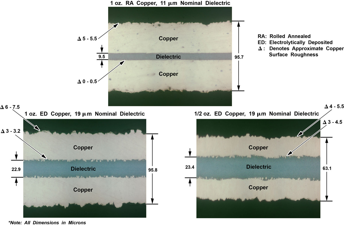
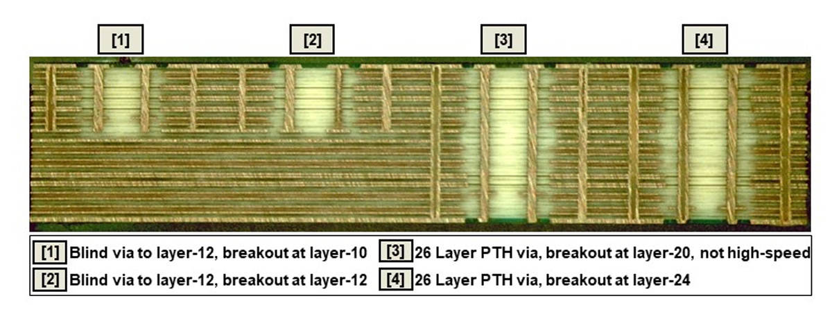
X-Section Examples
Information updated Tuesday, November 23, 2021
Any use of this site constitutes your agreement to the Terms and Conditions and Privacy Policy linked below.
"Mayo," "Mayo Clinic," "MayoClinic.org," "Mayo Clinic Healthy Living," and the triple-shield Mayo Clinic logo are trademarks of Mayo Foundation for Medical Education and Research.