Prior to performing any simulations, the SPPDG must first obtain or generate models of the discrete devices, integrated circuit devices and corresponding packaging. Whenever possible, the SPPDG obtains existing models and verifies them for accuracy. Nonetheless, the need to generate models arises in most efforts.
Fig.1 Flow chart of methodology used to derive an electrical model of a ball grid array (BGA) package using an empirical approach.
Because of the large variety of packaging technologies available, the SPPDG must develop packaging models using a wide range of techniques. For low frequency applications, lumped element models are generally adequate. When possible, the SPPDG develops lumped element packaging models with two different approaches, comparing the results for validity. In a theoretical approach, a model is developed using electromagnetic (EM) simulators like those developed at Mayo and/or available commercially, using the material properties and physical dimensions of the packaging interconnect, planes, dielectrics, etc. In an empirical approach, lumped element parasitics are measured in the SPPDG's state of the art test laboratory. When the two approaches agree, then the resulting model is used with confidence.
For more complicated and higher frequency packages, which require distributed-element models, the theoretical approach described above is used to generate a suitable model. For cases where the "as designed" material dimensions are either not available or suspect, a more involved process utilizing tools in the SPPDG clean room is required to develop an accurate model. In some cases, X-ray images are taken of the package to gain insight to the inner structure. If the X-ray image is not adequate, the packages are lapped down slowly to reveal the metal patterns, layer by layer. The layer patterns and geometries are then used in conjunction with cross section images taken with a scanning electron microscope (SEM) or transmission electron microscope (TEM) to develop a complete package model using EM modeling tools.
Fig.2 Scanning electron micrograph (SEM) of multilayer ceramic package cross section revealing critical dimensions.
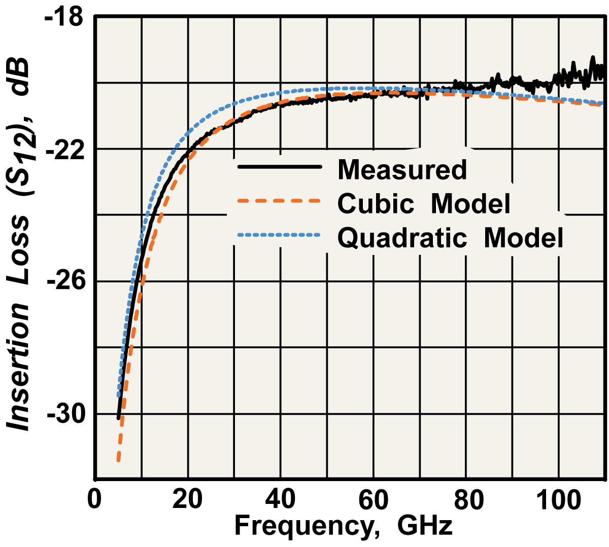
Whenever possible, the SPPDG validates its packaging models by comparing the simulated performance of the resultant models to measured data in the time and/or frequency domains from representative packaging.
The SPPDG can also generate individual transistor models from measured or simulated data, or we acquire these models from the integrated circuit fabricators, or less often, from the package vendors. The measured data can either be obtained from the fabricator of these devices or through measurement of the devices in the SPPDG test laboratory using commercial tools or software developed at Mayo. The commercial tools are also used to extract model parameters from both DC and high-frequency measured data. These tools are industry standard and can generate models for nearly every integrated circuit technology with which the SPPDG is involved.
As integrated circuit power densities have increased dramatically as transistor dimensions shrink and on-chip transistor densities increase, chip power dissipation levels have increased dramatically. As a result, we have relied increasingly on commercial thermal and thermo-mechanical modeling tools. However, because these tools are not yet complete, we have developed custom thermo-mechanical software models and physical models to ensure that appropriate cooling approaches are created for these very high power-density systems. At the time of this writing, descriptions of several of these models are being prepared for publication.
Information updated Wednesday, November 17, 2021
Any use of this site constitutes your agreement to the Terms and Conditions and Privacy Policy linked below.
"Mayo," "Mayo Clinic," "MayoClinic.org," "Mayo Clinic Healthy Living," and the triple-shield Mayo Clinic logo are trademarks of Mayo Foundation for Medical Education and Research.